The focus of this activity is developing radio frequency (RF) and mm-wave analogue components and circuits incorporating sensors aiming at increased complexity, higher power (using wide bandgap semiconductors) and exploring future transparent and flexible electronics for high frequency. Application are mainly in near future wireless smart systems, radars and other more than Moore approaches. Within this activity smart sensors for biomarkers are also explored.
Research Topics
Electromagnetism has a profound effect on our lives since applications such as wireless and satellite communications, space, airborne or ground active array radars, cable TV, and smart automotive infrastructure all depend on it. All of them are in continuous need of components with improved performance at higher power & frequency, smaller footprint & volume, with increased functionalities and at a lower cost and enhanced reliability. Novel solutions need to be sought to enable the next-generation of products with the efforts focusing on RF front ends (transceivers TRX modules) which are the key electromagnetic component that allows emission and reception of electromagnetic waves. Currently such innovative technologies are GaN based electronic components (high power capacity, low noise, chemically and thermally robust) and RF Microelectromechanical switches (MEMS) (lower insertion loss, higher isolation, greater power handling).
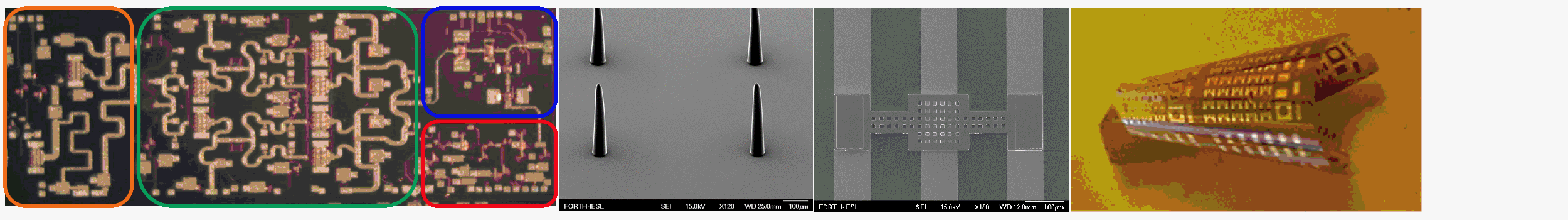
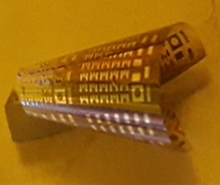
MRG in collaboration with Thales SA (France) has been developing technologies for the monolithic integration of GaN based Monolithic Microwave Integrated Circuits (MMICs) with RF MEMS focusing more on what is termed “coplanar approach”. MRG has already developed GaN based coplanar high power transistors operating in the X-band exhibit performances at par with commercially available “microstrip” ones such as the UMS GH25 transistor. MRG is currently attempting to set up a pilot line for the production of such RF front end modules.
Starting around 1970, Surface Acoustic Wave (SAW) devices were developed for pulse compression radars, oscillators, and band-pass filters for domestic TV and professional radio applications and recently for mobile or satellite communication systems. The shift of the resonance frequency of a SAW resonator, as effect of change of various physical parameters (temperature, pressure, mass loading, etc.) make these devices very useful in sensing applications. The traditional materials (quartz, langasite, langatate) used in SAW resonators manufacturing have excellent piezoelectric properties but they have also the disadvantage of their limited operating frequency, which remains normally below 2 GHz. Lately, the amount of data transmission in wireless network systems is increasing and the demand for SAW devices operating at frequencies around 5 GHz becomes important. Also in sensor applications, the sensitivity increases with the resonance frequency, being proportional with the square of the resonance frequency for mass, humidity and gas sensors. According to the wave mode there can be waves of Rayleigh, Lamb or a combination of both category. Wide bandgap (WBG) materials like GaN and AlN have very good piezoelectric properties and significantly higher acoustic velocities and are increasingly used for acoustic devices.
For over a decade, MRG has been developing SAWs, Film bulk acoustic resonators (FBARs) mainly for temperature, pressure and humidity sensing, Lamb resonators for biosensing (e.g. protein detection) and UV photodetectors. Key parameters are the developed micromachining process for extremely thin GaN membranes (below 500nm) and the electron beam lithography protocols for extremely narrow and densely packed interdigitated transducers (IDTs) as thin as 100nm with 100nm period.
This activity has resulted in more than 15 publications in established journals with citations in the range of 600 and in numerous conference presentations.
Acoustic sensors: For over a decade, MRG has been developing SAWs, Film bulk acoustic resonators (FBARs) mainly for temperature, pressure and humidity sensing, Lamb resonators for biosensing (e.g. protein detection) and UV photodetectors. Key parameters are the developed micromachining process for extremely thin GaN membranes (below 500nm) and the electron beam lithography protocols for extremely narrow and densely packed interdigitated transducers (IDTs) as thin as 100nm with 100nm period.
EEG sensors: Within the past 5 years, MRG has developed a dry microneedles based Electroencephalogram (EEG) electrode with simple fabrication involving just a single lithography step without the use of “sacrificial” substrates. The resulting process is therefore simpler and of lower cost.
Gait sensors: MRG as part of a Greek collaborative effort, is working towards the design and manufacture of a smart, wearable insole (Smart Insole) with built-in pressure measurement sensors, other micro-electronic sensing elements and communication devices to tackle the challenge of efficient gait monitoring in real life. This wearable insole is based on unique layer that consists of a polymeric material with embedded piezoelectric flakes, an inertial measurement unit including a triaxial accelerometer, gyroscope and magnetometer to capture the gait characteristics in motion.
Future RF systems are in continuous need of components with improved performance at higher power & frequency, smaller footprint & volume, with increased functionalities and at a lower cost and enhanced reliability. Aggressive miniaturization is the key requirement for future RF Transceiver (TRX) systems. In order to achieve, there is a need to transform current TRX 2D architecture into 3D heterogeneously or sequentially integrated one.
MRG conducts research in III-nitride based MMIC, III-nitride based sensors and RF MEMS and has already demonstrated the monolithic integration of MMICs with RF MEMS. A major advantage of III-nitride based acoustic sensors is the possibility of monolithic integration with other active and passive circuit elements, enhancing the future development of smart microsystem technological platforms on this material. In particular MRG is working on the idea of “all-in-Gallium Nitride” solution involving MMICs, RF MEMS, multimodal sensors supported by disruptive nanotechnologies such as 1D &2D materials, which will deliver a single transceiver component which will radically transform the current 2D TRX architecture into a 3D System in Package (SiP).
Transparent and Flexible electronics are part of the Key Enabling Technologies of Nanotechnology, Advanced Materials, Photonics and Micro-Nanoelectronics. Flexible and transparent electronic devices and systems can find applications in the high growth market sectors of healthcare, smart packaging for food and pharmaceutical products security, human-machine interfacing, sensor networks, automotive electronics, the Internet of Things, flexible displays, wearable gadgets and other emerging chip markets.
The activity on flexible and transparent electronics within MRG employs low temperature PVD deposition techniques like rf sputtering and rf magnetron sputtering for fabricating n-type and p-type nanostructured oxides, nitrides and oxynitrides like ITO-N, ZnO-N-Al, Ir, NiO-Al, TaO-N, ZnSnO, CuO, etc, with controllable properties and long term stability, on flexible substrates (PET, glass, etc). By making use of innovative and low-cost fabrication-approach devices, TTFTs, photo-transistors, transparent diodes and transparent PVs are developed.


Heads


Technical Staff


Research Associates

Alumni

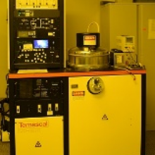
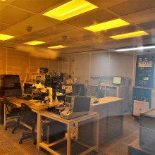
Infrastructure Equipment
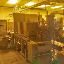
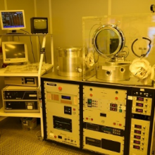
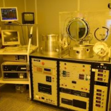
Molecular Beam epitaxy system by VG 80H with automated control.
- Capable of handling up to 3" substrates
- RHEED 15KeV system
- Mass spectrometer 1 - 300 amu
- K-cells for Galium (2), Aluminum (2), Arsenide, Indium, Silicon and Berilium
UHV e-beam evaporator with an 8 target turret and in situ ion beam cleaning system.

Two thermal evaporators (Home-made)

RF diode and RF magnetron sputtering system with 3 electrodes.
Reactive Ion Etching system (Vacutec 1500) with in situ laser interferometry and optical emission spectroscopy end-point detection techniques (Jobin Yvon Sofie)

Inductively Coupled Plasma Etching system (Oxford Plasma Pro 100 Cobra)
Plasma enhcanved CVD system (Plasmatherm Vision 310 PECVD) with stress control of Si3N4 achieved by using mixed-frequency deposition or low-damage He dilution.

Atomic layer deposition (Picosun R-200 Advanced) with sources for Aluminum oxide and Hafnium oxide deposition capability) + Ozonator (InUSA AC Series Ozone Generator)

Programmable 3-stage tube furnace (Carbolite)


Two programmable hot plates with vacuum (UniTemp GmbH VHP-210-160)

Two programmable spinners up to 6” (Suss MicroTec LabSpin 6BM)

Electron beam writer attachment (Raith Elphy Quantum) for the field emission SEM (Jeol 7000F)


Programmable horizontal tube (3”) furnaces up to 1200°C (ELITE Thermal Systems Limited TMH12/75/750)


Semiconductor Characterisation System (Keithley K4200):
- Two SMUs (max 0.1A, max 210V, 2W)
- High power SMU (1A, 210V, 20 W)
- DC and pulsed measurements ( 500 ns minimum pulse width)


