This activity focuses on energy handling and recovery. The focus is on functional materials for smart glasses and zero energy buildings, next generation, high efficiency III-N photovoltaics and nanowire solar cells, as well as high power, high voltage (KVolt) SiC based electronics for grid power management.
Research Topics

With an increased awareness on environmental issues and to compete with COP21 Paris agreement, there is a challenge for physicists, chemists and engineers to develop new products, processes and services that can achieve critical societal, economic and environmental objectives. Green Technologies and Green Engineering are the answers to that challenge and these are the issues this activity is trying to tackle.
It is known that for minimizing energy in buildings (which are responsible for 35-40% of total final energy consumption) and using eco-sustainable resources, the design and development of high performance self-powered user-controlled smart window systems based on functional strongly correlated materials, oxides and solid-state electrolytes can enhance solar and thermal management of buildings, transportation means, etc. The development of such functional materials on flexible substrates (PET, glass, etc) can subsequently be mounted on a carrier glass with its proprietary bonding solution and provide energy saving in old buildings (retrofits), etc.
The activity on functional materials for smart and energy autonomous glasses & windows within MRG employs low temperature PVD deposition techniques like rf sputtering and rf magnetron sputtering for fabricating bio-inspired thermochromic coatings (VO2-based), energy autonomous solid-state electrochromic devices (WO- and NiO-based) and transparent photovoltaics and thermoelectric generators.
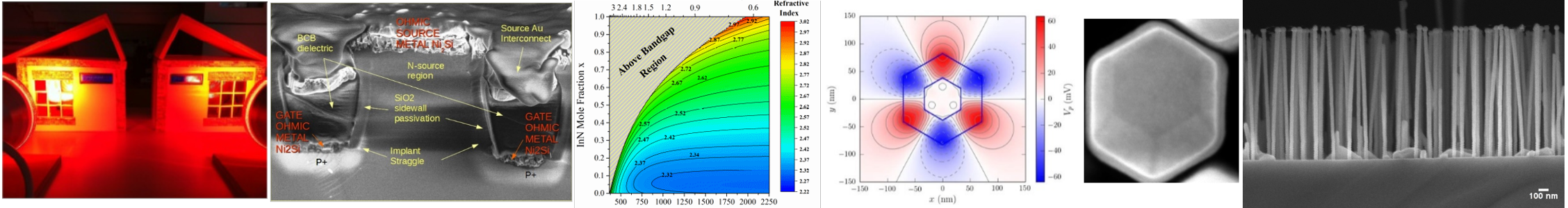
Power transistors based on wide band gap semiconductors are subject of intensive research the last decade. The high current and high voltage capabilities of these devices, largely exceeding that of Si devices, represent a challenge on various aspects related to the device fabrication, characterization and packaging. JFETs have the lowest overall losses of switching devices and their fabrication process is quite straight forward. The main drawback with VJFETs is that they are usually normally-on (depletion mode), which is considered unsafe in power applications. Moreover, JFETs are very robust devices with a channel not seriously affected from surface effects. This was the reason for developing SiC JFETs at FORTH.
The appropriate JFET geometry is significant: The usual 4H-SiC JFETs are either purely vertical (VJFETs with Static Induction Transistors-SITs operation) or Semi-lateral (SLJFET). Optimum SLJFET fabrication requires two-step implantation and re-epitaxial growth after material etching on specific locations. Trenched VJFET requires only one implantation step and the fewer lithography steps. The only difficulty is the tight control of the dimensions, which are of the order of 1-2 μm for both source pillars and gate pitch arising, thus, an issue of tight registry control. For the above reasons, the trenched and implanted TI-VJFET have been chosen.
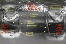
The III-Nitride semiconductors and in particularly InGaN alloys have a tremendous potential for high efficiency/lower cost next generation earth and space photovoltaics, due to their direct bandgap extended range, polarization fields and high radiation and chemical resistance. However, despite international efforts for more than 10 years this potential has not been realized. Based on MRG’s unique know how for state-of-the- art epitaxial InGaN materials we aim to address bottlenecks and substantiate their photovoltaic potential. With suitable for photovoltaic applications characteristics, state-of-the-art InGaN thin films have been realized in the entire composition range and their optoelectronic properties were accurately evaluated. Particular emphasis was given to avoid compositional fluctuations that act as potential minima to trap photo-generated carriers. The traditional approaches to III-N p-i-n solar cells have been examined and it was revealed the important role of polarization field in opposing efficient carrier collection. Therefore new design approaches based doping-polarization engineering has been implemented and extended device simulation, based on experimental material parameters, were employed to optimize parameters for maximum conversion efficiency in single n-InGaN/p-GaN heterojunctions and tandem n-InGaN/n-p Si junctions. Novel device processing approaches have been investigate to address specific bottlenecks problems in device realization.
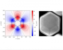
In the quest for next generation photovoltaic technology, nanowire solar cells attract wide interest for two reasons. First, the enhanced light absorption of nanowire arrays, based on their anti-reflecting properties, light trapping and resonant waveguiding effects, allows for an order of magnitude reduction in the amount of materials, needed for an efficient solar cell. Second, due to their large surface/volume ratio, nanowires exhibit relaxed lattice-mismatch requirements allowing for high quality nanowire growth on less costly substrates (e.g. GaAs nanowires on Si). Recently, a conversion efficiency of 15.3% has been demonstrated using GaAs nanowires, underlining their potential to compete with other solar cell technologies. A critical parameter in fabricating a nanowire solar cell is the uniformity of the nanowire array. This issue is typically addressed by pre-patterning the substrate in order to trigger simultaneous nucleation of the nanowires. This pre-patterning step, however, adds to the complexity and cost of fabrication of the nanowire arrays. In this project, we have devised a new method producing highly uniform GaAs nanowire arrays on unpatterned Si substrates. The method consists of a controlled chemical oxidation process to replace the native oxide on Si(111) substrate with a reproducible chemical oxide.

Heads


Technical Staff


Alumni