This activity is part of the Micro-electronics Research Group, the activity focuses in semiconductor material aspects and physics of heterostructures and nanostructures. Molecular beam epitaxy for semiconductor devices is the primary focus including III-V (Nitride and Arsenides) studying the physics and interaction of material and component in nanowires, FinFETs, growth and properties of ternary compound semiconductors and novel heterostructures for use in beyond-Moore applications.
Research Topics
Molecular Beam Epitaxy (MBE) is an ultrahigh vacuum technique that offers atomic-level control in the epitaxial growth of semiconductors on crystalline substrates. MBE is applied in the epitaxy of III-V semiconductors to create artificial semiconductor materials that combine layers of different semiconductors, i.e. they comprise semiconductor heterostructures. III-V heterostructures provide the means to vary the electronic and optical properties of a semiconductor along its growth axis and to realize the desired spatial variation (profile) for the energies of electrons and holes, the refractive index and absorption coefficient. Such planar heterostructures are used to implement all modern III-V nanoelectronic and optoelectronic devices, with key examples being the High Electron Mobility Transistor (HEMT) and Multiple Quantum Well Laser Diode (MQW-LD). The formation of heterostructures along 2 or 3 dimensions becomes possible by exploiting MBE growth mechanisms and allows to experimentally realize nanostructures of nanowires and quantum dots, respectively. In addition, heteroepitaxy on a foreign substrate enables the realization of semiconductor materials non-existing as bulk crystals, as well as the combination of different semiconductor materials/technologies on the same substrate (monolithic integration). Our III-V MBE related research spans from fundamental studies on growth mechanisms, heterostructure material properties and physics, to the development and optimization of growth processes for various types of III-V semiconductor devices and monolithic integration applications. The work is supported by electro/optical modelling for optimizing the design of the III-V nano-heterostructures, as well as their experimental validation by fabrication and evaluation of semiconductor devices, which includes research on the basic device fabrication processes (e.g. surface passivation).
Recent and current research areas of interest include, but not limited to:
- Polarization induced carriers in III-Nitride heterostructures
- InN thin films, nano-heterostructures and Field-Effect Transistors (FETs)
- AlN/GaN HEMTs for high frequency devices and power switches
- III-Nitride heterostructures on single crystal and polycrystalline diamond
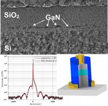
- Monolithic integration of III-Nitrides and III-Arsenides on Si
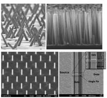
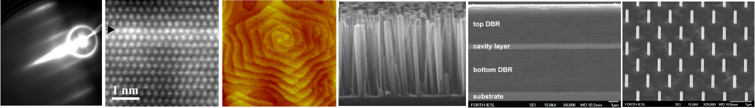
The semiconductor nanowires are one-dimensional crystals with typical length in the range of micrometers and diameter in the range of nanometers. The geometrical characteristics of semiconductor nanowires result to unique physical and chemical properties for nano electronic, photonic and sensing applications: (a) defect-free lattice-mismatched heterostructures, (b) well defined conductivity nano-channels and (c) high surface area for chemical interactions and efficient light extraction or absorption. Semiconductor nanostructures resembling to nanowires, lying horizontally on a substrate surface, are also the fins (nano-walls). Both the semiconductor fins and nanowires define conductivity nano-channels for Field Effect Transistors (FETs) that can be efficiently modulated by a gate electrode that surrounds the three sides (tri-gate) or all sides (all-around gate) of a fin or nanowire, respectively.
Nanowires based on III-V semiconductors are particularly promising, since many III-V compounds exhibit high electron mobility and drift velocity and efficient light emission and absorption. They can be used in the ultimate nanoelectronic FETs for digital applications, but also in other devices, such as nano Light Emitting Diodes (LEDs), integrated on Si substrates. III-V heterostructures within the nanowires can provide band discontinuities and potential barriers for additional means of carrier confinement and quantum effects’ realization.
Our research aims to develop fundamental understanding and knowhow for the formation, physical properties and applications of III-Nitride (GaN, InN, AlN) semiconductor nanowires and fins. We investigate their formation by both bottom-up and top-down processes. The bottom-up approach is based on spontaneous epitaxial growth of III-N nanowires by Plasma-Assisted Molecular Beam Epitaxy (PAMBE), whilst the top-down approach employs etching of planar semiconductor layers/heterostructures. Substrate nano-patterning techniques are used for selective area formation of III-N nanowires. We develop device nanofabrication technologies with generic application potential, using two challenging platforms:
- GaN vertical nanowire field-effect transistors (NW-FETs)
- GaN fin filed-effect transistors (FinFETs).
These technologies could be adapted to different GaN transistor applications (digital, RF, power switching), as well as to other types of III-Nitride nanowire devices.
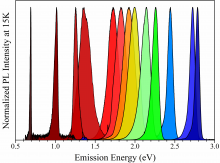
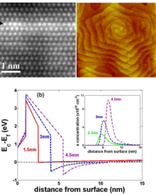
Indium-Gallium-Nitride (InGaN) alloys are of particular importance in advanced optoelectronic and photovoltaic applications due to the direct bandgap spanning the 0.7 to 3.4 eV energy range. However, a number of bottlenecks (thermodynamic immiscibility, large lattice mismatch, complex epitaxial growth) limit the development of high quality material in the entire compositional range. The aim is to study in depth epitaxial growth processes, take advantage of RF-MBE “far from equilibrium” character and develop device quality epitaxial thin films and heterostructures with alloy ternary composition in the entire composition range.
III-Nitride nanostructures pose a set of unique properties (large bandgap differences, strong polarization, specific band alignment to Si and other semiconductors) that open many possibilities for novel functional applications. Our aim is to develop basic technology to enable those applications and explore their characteristics. Non-traditional epitaxial nanostructures approaches, such as development of III-N quantum dots structures embedded in dielectric materials, patterned epitaxy, as well as, novel heterostructure designs and doping-polarization engineering has been explored to realize devices with new functionalities or enhance device operation. Within this context the possibility of III-N semiconductor QDs floating gates for non-volatile memories with large voltage threshold and 10-years retention and room temperature negative differential resistance characteristics in double barrier RTDs have been demonstrated.
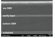
Semiconductor microcavities are nanostructures grown by Molecular Beam Epitaxy, which consist of either GaAs or InGaAs Quantum Wells embedded between two Bragg mirrors forming a planar Fabry-Perot cavity. In such structures, exciton polaritons result from the strong coupling between a resonant optical cavity mode and confined excitons. The bosonic nature of exciton polaritons inherited from their light–matter composition is responsible for observations of stimulated scattering, amplification, condensation and lasing of polaritons. In contrast to conventional lasing, where coherent light emission is driven by stimulated photon emission, polariton lasing is achieved through the stimulated scattering of polaritons and the formation of a condensate without the need for population inversion. Therefore, polariton lasing promises two orders of magnitude lower threshold than conventional photon lasing and a new generation of ultralow threshold laser devices. In addition, polariton condensates have been shown to exhibit similarities to atomic Bose–Einstein condensates (BECs), displaying a spontaneous build-up of long-range spatial coherence and a thermalized distribution within the population. Unlike atomic BECs, polariton condensation can be achieved at high temperatures due to the very small polariton effective mass. Major prerequisite to all the above observations is the ability to fabricate state of the art MBE grown high finesse microcavity structures allowing very long polariton lifetimes capable of supporting efficient relaxations of polaritons to the ground state and formation of condensate. Other important challenges include growth of p-i-n diode microcavities for efficient electrical injection of carriers while preserving finesse of the grown structures.
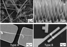
The purpose is the investigation of SiC nanowires (NWs) for logic and bio applications. The main target for the former is the demonstration of the viability of using SiC NWFETs as an alternative technology to the Si ones. Our previous theoretical studies on the 3C-SiC NWFETs, in various transport regimes have shown that the SiC NWFETs have similar performance to the Si-based ones while they offer the advantage of high temperature operation and eventually efficient heat dissipation. Thus, the use of SiC NWFETs will not degrade the electrical characteristics while it will address main issues in device scaling. Up to now, the potential advantages of SiC-based NWs have not been demonstrated. The main proposed causes were the poor material properties of the grown materials (high density of planar defects and high residual doping) and the basic technology employed for fabricating SiC NWFETs resulting in poor quality interface with gate dielectrics. Top-down NWs have been used for the SiC NWFETs fabrication on the basis of low-doped 3C-SiC material and eliminating, thus, the first reason. The transistors with top-down grown NWs exhibited three orders of magnitude higher current and transconductance values with respect to SiC NWFETs with bottom-up grown NWs. Nevertheless, it was not possible to switch-off the transistors showing the importance of interface with the gate dielectrics. The current effort is to develop the technology for demonstrating Gate-All-Around (GAA) devices with NW diameter lower than 80nm. Towards this aim, two different lithography techniques are employed. E-beam lithography and Nanoimprint lithography.
Heads


Scientific Staff

Technical Staff


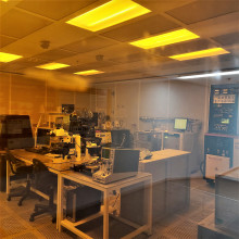
Infrastructure Equipment
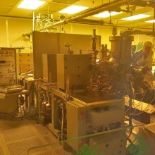
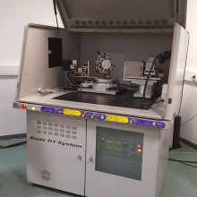
Molecular Beam epitaxy system by VG 80H with automated control.
- Capable of handling up to 3" substrates
- RHEED 15KeV system
- Mass spectrometer 1 - 300 amu
- K-cells for Galium (2), Aluminum (2), Arsenide, Indium, Silicon and Berilium

- Main Chamber for up to 3" substrates
- Transfer chamber
- Entry-outgas chamber
- K-cells for Ga, Al, In, Si
- Si sublimation source
- RHEED 15 KeV system
- Mass spectrometer 1-200 amu
- N2 RF plasma source
- Source alteration possibilities, e.g. gas injector for NH3
Field Emission Scanning Electron Microscope (FE-SEM) (Jeol 7000F)
- Energy Dispersive X-ray Analysis (EDX) (INKA, Oxford Instruments)