The PPM group is in the last 15 years on the forefront of the metamaterials research (with the term metamaterials to include here also photonic crystals and plasmonics - as engineered composite materials). It collectively has been, and continues to be, a prime mover and initiator of the development of one of the main categories of metamaterials, that of left-handed metamaterials (i.e. metamaterials characterized by both negative electrical permittivity and permeability values, and thus negative refractive index). The revolutionary concept of negative refractive index originally prompted objections, based on perceived violations of causality, momentum conservation, and Fermat’s principle.
Research Topics
Research Topics
|
Left-handed materials (LHM) are composite materials whose properties are not determined by the fundamental physical properties of their constituents but by the shape and distribution of specific patterns included in them. LHM have the unique property of having both the effective permittivity and the effective permeability negative. The aim of the research is the theoretical understanding, analysis, development, fabrication and testing of left-handed materials (LHM), and also the investigation of their feasibility for applications.
A very interesting question is whether the negative index of refraction property can be implemented at optical frequencies. The phenomenon of negative refraction has recently been predicted by numerical simulations on dielectric, photonic crystals, at certain frequencies near negative group-velocity bands. Although the refracted beam may bend toward a negative angle in these systems, it is difficult to define an equivalent index of refraction with the same generality as we find in LHM materials, because these effects cab be interpreted as higher order Bragg reflection peaks. Furthermore, surface waves at the interface between photonic crystals and other uniform media complicate the surface matching problem, making design considerations more difficult. Nevertheless, the use of photonic crystals as negative refractive materials is intriguing and may offer the means of extending the phenomenon of negative refractive index to optical wavelengths. Any material that exhibits the property of negative refractive index, a property not observed in naturally occurring materials, will have a variety of practical applications.
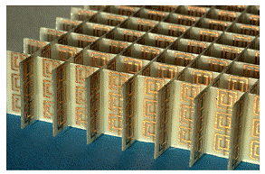
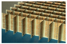
Photonic crystals are a class of artificial periodic composite materials which exhibit electromagnetic band gaps (i.e. frequency regimes where the EM waves can not propagate). This band gap property makes the PCs very important for the manipulation of EM waves; they can act for the EM waves in the same way as the semiconductors for the propagation of electrons; e.g., formation of proper defects leads to localized light modes with desired properties, like guiding of light (by creating linear defects in PCs – see next figure), storing light in point-like defects etc. All this ability for light manipulation can be used to improve the functionality of existing light emitting, receiving and propagating devices, to produce novel, optimum devices, making even possible the creation of integrated circuits fully photonic.
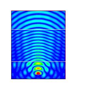
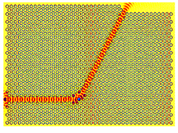 Guiding and bending of light through a two-dimensional photonic crystal waveguide with a bend. Our tasks in the PC research include study of various PC-based structures and identification of structures that can be used as components for the creation of PC integrated circuits; also, exploration of the interaction of sources with finite PCs, study of defects in PCs, left-handed behaviour of PCs etc.
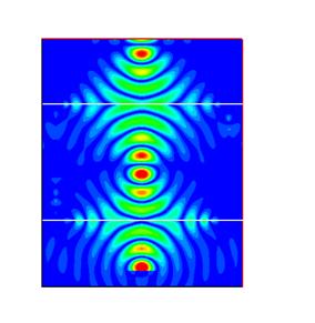
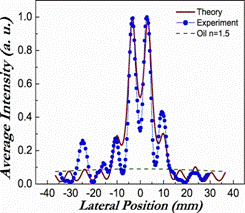
Phononic crystals are the acoustic analogue of photonic crystals. It is going for periodic composite media with spectral regions where the propagation of the acoustic  and elastic waves is forbidden (phononic band gaps). Phononic crystals have for the acoustic and elastic waves all the manipulation capabilities that photonic crystals have for light. Their most important application is in the creation of acoustic filters, as the richness in parameters of the acoustic systems gives the ability for very wide band gaps. Our current topics on the phononic crystal research include combination of phononic and photonic band gaps in the same system for the creation of opto-acoustic devices, characterization of self-assembled colloidal crystals made of core-shell particles (which can give band gap in sub-wavelength regimes) and optimization of their properties, negative refraction effects in phononic crystals etc. 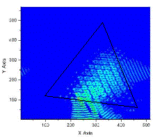   Negative refraction in a phononic crystal. The crystal has the shape of the triangle.
The aim of the present research is the theoretical understanding of the properties of disordered systems, with emphasis on light localization and random lasers.
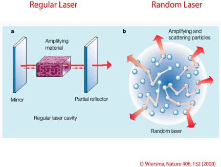 Random Lasers Random lasers are a combination of strongly scattering media and an optical gain medium. Â These systems have many features in common with conventional lasers based on an optical gain medium enclosed in a cavity with two mirrors to enhance stimulated emission. Â In random lasers, multiple scattering plays the role of the mirrors (see the figure in the beginning). Â For example, threshold behavior for lasing action and frequency narrowing has been observed in random lasers. Â Evidently, the optical properties of random lasers are quite different from conventional lasers; the propagation of pump and fluorescence light is diffusive, and the absence of a well-defined cavity with modes along its axis, there is no “preferred direction” in feedback and loss processes. Â The ambiguity as to what exactly constitutes the loss of a random laser, how optical feedback works if it is “omni-directional,” and the theoretical prediction of an intensity divergence have led a continuous debate about what happens at, and above, the laser threshold. Â We have developed a dynamical approach for understanding the properties of random lasers, especially above the laser threshold. We plan to collaborate with experimental groups at Amsterdam and IESL-FORTH (Laser group) to understand the dynamical behavior of the random laser systems and check our recent predictions about the shape of the wavefunctions of random lasers and low threshold lasing in periodic and/or random materials. It is expected that in the case of a 3d PBG material, the random feedback effects will be considerably stronger, and can give lasing with a much lower threshold. We plan to use the inverse opal structures fabricated at the University of Amsterdam to check these ideas. We plan to investigate the emission spectra of dopants (such as Erbium) inside 3d photonic crystals. Â The situation is reminiscent of atoms or molecules in 1d Fabry-Perot cavities. Â The main difference between Fabry-Perot cavities and photonic crystals is that PC acts as 3d cavities, thereby promising complete control over emission. These studies will help us develop low threshold lasers and light-emitting diodes using photonic crystals. One of the current challenges in laser optics is to take advantage of the resonant modes within particles to obtain high quality micro-cavities with low threshold. We have presented a study of the effect that the internal resonances of individual particles play on the emitted intensity, and demonstrated how optimal tuning of the size and distances between the particles can enhance the quality factor by more than 4 orders of magnitude. The potential applications of this work on the design of an optimal mirco-cavity and on a random laser are essential. Light Localization The analogy between the propagation of electron waves and classical waves has led to a revival in the research of the transport of light in disordered scattering systems. The final goal of many of these studies has been to observe the optical analogue of Anderson localization in electronic systems. Â Experimental difficulties in realizing a random medium where the optical absorption is low enough and the light scattering is efficient enough to induce localization has been the reason why, for a long time, only microwave localization was realized. Â In light localization experiments, the absorption is large and, therefore, complicates the interpretation of results. We plan to carry out new experiments at the University of Amsterdam in very strong scattering media to clearly distinguish between the effects of optical absorption and multiple scattering. Â The effects of finite size and internal reflection at the boundary of the sample should be also included appropriately. Currently, experiments are in progress with powders of semiconducting materials such as Si, Ge and GaP at frequencies near and below the semiconductor gap of these materials. In addition, a unique porous form of GaP has recently been developed as well-defined random sample with a connected network topology. The difference in topology of powders and network structures and its consequences in localization behavior are still under study both experimentally and theoretically. To characterize the wave propagation of light in random media, a variety of optical techniques have been developed. Â In particular, the dependence of scattering properties such as the mean free path as a function of sample thickness, the enhanced backscattering profiles and speckle correlation techniques have proven to be essential to augment the static measurements with time dependent techniques to determine the dynamical transport properties. Â For example, short optical pulse transmission measurements are able to determine the dynamical diffusion constant and properties such as the effective energy and phase velocity in the medium. We will use the Energy Density Coherent Potential Approximation developed by K. Busch, E. N. Economou, Maria Kafesaki and C. M. Soukoulis, to obtain better estimates for the optimum topology and scatter characteristics. We also plan to develop the theory of pulse transport in disordered systems and will be in close contact with the group of Professor Ad Lagendijk at the University of Amsterdam, which recently moved to University of Twente. Nonlinearities Nonlinear dielectric materials exhibiting a bistable response to intense radiation are key elements for an all-optical digital technology. We have used our FDTD methods to study the time-dependent switching properties of nonlinear systems for constant wave illumination. The conditions for a fully controlled and reproducible switching were obtained. Our FDTD methods were also used to study the effects of disorder on the width of the photonic gaps. It is found that the gaps can survive a strong amount of disorder. It looks like that short-range order is needed to have a gap in a photonic crystal. In summary, fascinating novel science and technology can be expected from the synergy of the fields of light localization, photonic band gap materials, and random lasers. Photonic crystals offer innovative ways to manipulate light not possible in any previously known photonic material. They represent the “semiconductors of the future,” and may become the focus of the photonics revolution of the twenty-first century. |


Research directions / Objectives
The Transparent Conductive Materials (TCM) Group has an accumulated experience of more than 25 years in composing new materials (powders, films) while using a wide range of characterization techniques. Particularly the TCM group is working on the development and synthesis of new Metal Oxides Nanomaterials (for Sensing, Optical, Optoelectronics, Electronic, Photochromic and Photo-Catalytic applications) for:
- Development of a new type of metal oxide Gas Sensors for environmental mainly monitoring indoor air quality (iAQ). Study the gas sensing properties of different materials
- Reducing Gas Molecules (e.g. CO, H2, CH4, ethanol, propane)
- Oxidising Gas Molecules (e.g. NO2, O3, SO2, Cl2)
- Synthesis of Innovative Photo-Catalysts for air (indoor/outdoor) and water depollution as well as bacteria disinfection which can effectively be activated under UV and particularly visible light.
- Development of n- and p-type Metal Oxides of TCOs and ASOs
- Transparent Thin Films Transistors (TTFTs) for transparent Electronics
- Flexible Electronics on PET, PEN substrate
- Development of Electrochromic/Thermocromic materials and devices
- Hydrophilic / Hydrophobic self - cleaning surfaces for House – hold applications
In detail, the TCM group has a very successful track-record on:
Metal-Oxide (MO) gas sensing materials and devices highlighted by ultra-low detection limits for gases such as O3 and NO2 in the low ppb range at room temperature at world record levels (i.e. <10ppb for O3 , <0.5ppm for NO2 )Photo-Catalytic materials / transition metals undoped/doped for IAQ control
- Degradation of Dye’s (set- up by ISO standards to measure the photocatalytic degradation in Methylene Blue, Methyl Orrange, Rhodamine 6G and others)
- Degradation of inorganic compounds (NOx, SOx, ….) and Volatile Organic Compounds, VOCs (formaldehyde, acetaldehyde, benzene, toluene…)
Heads


Research Associates

Students


Alumni
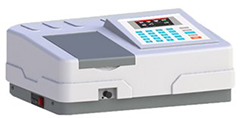
High quality measurements can be performed using the K-MAC UV-Visible spectrometer which connects to light sources, cuvettes and other accessories and covers the 220-800 nm range.
The K-MAC UV-Vis, equipped with several types of optical fibers, is a miniature spectrometer preconfigured for general UV-Vis measurements from 220-800 nm. It consists of a spectrometer (detector), light source, cuvette holder and other accessories. Using this spectrometer, we can measure different modes (absorbance & transmittance, fluorescence & reflectance, irradiance) by switching the light source location. This convenient, high-performance spectrometer fits into the palm of your hand, giving your measurements new flexibility. Using the modular approach, we can customize each measurement with our wide array of sampling accessories and light sources.
Our BIOBASE BK-D590 Double Beam Scanning UV/VIS Spectrophotometer, gives us the possibility to characterize several solid or liquid samples in absorption, transmission, or reflection mode, covering a spectral range of 190-1100nm, using a 1200 lines/mm grating.
- Spectral bandwidth: 0.5,1.0, 2.0, 4.0, 5.0 nm
- Wavelength accuracy: ± 0.3 nm
- Wavelength repeatability: ± 0.2 nm
- Photometric Accuracy: ± 0.002A (0~0.5Abs), ± 0.004A (0.5~1.0Abs), ± 0.3% T (0~100% T)
- Photometric Repeatability: 0.001Abs (0~0.5Abs), 0.002Abs (0.5~1.0Abs), ≤ 0.2% T (0~100% T)
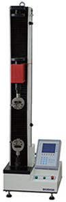
We have the possibility to measure the mechanical properties of several samples using a BIOBASE BKWW-5S universal testing machine, suitable for tension / compression and flexural tests, using standardized grips.
The BIOBASE BKWW-5S universal testing setup is applicable for a wide range of materials for tension, compression, bending, shearing and low cycle test. Moreover, BKWW-5S is suitable for metal, rubber, plastic, spring, textile, and components testing, following ASTM, ISO, DIN, GB and other international standards.
- Max. Load: 5kN
- Structure: Single Column Double Spaces
- Control Method: Single Chip Control
- Load Accuracy: 1 Class
- Load Range: 2 % ~ 100 % F·S
- Displacement Resolution: 0.01 mm
- Test Speed: 1 ~ 500 mm/min
We have the possibility to implement quantitative detection and mapping of chemical characteristics through spectral imaging using an XPECAM X01 Multispectral imaging system, equipped with a CMOS Monochrome sensor, covering 30 spectral bands, operating from 350 - 1200 nm, with a spatial resolution of 5M pixels.
XPECAM X01 exploits a wide range of wavelength bands across the near ultraviolet to the infrared wavelengths of the electromagnetic spectrum, allowing the study of materials, their deterioration, and extract spectral information at selected areas from 350 nm to 1200 nm.
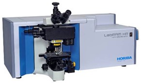
A Horiba LabRAM HR Evolution Raman microspectrometer (30 - 4000 cm-1), with open space microscope, offering a large free space under the objective turret. Thus, we can use large sample holders like cryostats, high temperature cells, high pressure cells, or just large samples. In order to get high stability, the sample stage is hard coupled to the LabRAM HR, while focusing is achieved by adjusting the height of the microscope objectives instead of the sample stage. This microscope offers all the functions of the standard microscope. It includes high throughput achromatic coupling optics optimized to work from UV to NIR with maximum efficiency, icluding also Open Electrode CCD air-cooled to -60°C, 4 objectives 10x (numerical aperture of 0.25), long distance 50x (NA=0.5), water immersion 60x (NA=1.2), and 100x (NA=0.9), and 2 gratings (600 and 1800 grooves/mm, respectively).
The Horiba LabRAM HR Evolution Raman microspectrometer is attached to two air-cooled solid state laser kits, at 532 nm (532 nm/100 mW), and at 785 nm (785 nm/ 100 mW).
Moreover, a Linkam PE120 thermoelectrically cooled stage is attached to the LabRam HR Raman spectrometer with a temperature range of -25°C to 120°C (heating/cooling rates of 0.1-20°C/min and a stability of ± 0.1°C/min).
- The LabRAM HR systems provide high spectroscopic resolution and a unique wavelength range capability that offers both great flexibility and high performance. They are widely used for standard Raman analysis, photoluminescence (PL), tip enhanced Raman scattering (TERS) and other hybrid methods.
- Photoluminescence (PL) measurements can be performed using the laser kits of the Raman spectrometer; The detection limit is given by the open Electrode CCD at 1050 nm.
- The unique high resolution mode is ideal for subtle band analysis such as that for phase (crystalline/amorphous), of proteins, weak bonding forces (such as hydrogen bonding) and semiconductor stress measurements – in fact most applications where it is important for the precise characterization of position or shape of the Raman spectral features. Band analysis with a resolution in the order of 0.3 cm-1 to 1 cm-1 is particularly suited to the high resolution mode. Its dual capabilities also enable more routine low/medium resolution Raman analysis and even broader band laser induced micro-fluorescence or luminescence to be conducted on the same bench-top instrument.
- The LabRAM HR has a true confocal pinhole with user controlled variable aperture. Unlike pseudo-confocal configurations (e.g., slit-binning methods) the confocal pinhole fully matches the laser spot and provides the highest spatial resolution with maximum signal throughput.
- Finally, the LabRAM HR spectrometer is equiped with a SWIFT FAST Confocal imaging system, suited for fast mapping applications (XY specifications: repeatability ≤ 1µm, accuracy ±3µm, resolution 10 nm; Z specifications : resolution 0.01µm).
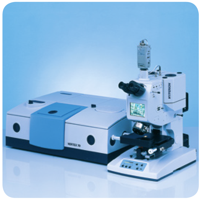
A Bruker Vertex 70v FT-IR spectrometer attached to a Bruker HYPERION 2000 FT-IR microscope allows us to perform Transmission/Reflection/Absorption measurements in a spectral range of 24000 - 10cm-1 (0.3-720THz), covering a wide frequency range from far IR to visible regime.
- Using the above FT-IR spectrometer, we can characterize thin films, powders or liquids, either under vacuum, or in ambient air.
- Transmission measurements can be performed at several angles of incidence, varying from 0˚ to 90˚.
- Reflection measurements can be done using the A 513/Q specular reflection setup at several angles of incidence, varying from 13˚ to 83˚.
- The Vertex 70v FT-IR spectrometer is equipped with a A225/Q Platinum ATR unit with single reflection diamond crystal which allows the infrared analysis of unevenly shaped solid samples and liquids through total reflection measurements, in a spectral range of 5500 - 10cm-1 (0.3-165THz), at temperatures up to 350°C.
- A Linkam FT-IR 600 heating and freezing stage with a temperature range of -196°C to 600°C and heating rates up to 150°C/min can be coupled to our Vertex 70v FT-IR spectrometer, or the HYPERION 2000 FT-IR microscope.
- Using both the spectrometer mentioned above, linearly (and circularly) polarized transmission (and reflection measurements) can be performed, from far IR to visible regime, using several sets of linear grid polarizers, or circular polarizers using super-achromatic quarter-wave plates with an accuracy of λ/4±14%.
- A Thermo Spectra-Tech High Pressure Vacuum chamber allows the exposure of the samples to extreme reaction conditions, at temperatures up to 900°C at ambient pressure, or at lower temperatures up to 400°C at up to 1500 psi, providing a stability of ± 1°C.
This way samples can be tested for various applications, such as:
- Control of sampling environment of solid samples
- In-situ measurements
- Adsorbate characterization
- Catalysis studies
- Dehydration kinetics
- Solid-solid phase transitions
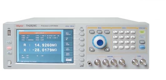
TH2829 LCR meter is an automatic component analyzer, which is completely appropriate for test requirements of all kinds of industrial and military standards. It is based on a well-designed measuring circuit and on optimized algorithms, which enhance further the test stability of low-D capacitance and high-Q inductors. The instrument is provided with 10V AC test level, 10V/100mA bias current and standalone 10V/50mA DC current, making it convenient for applying in the test of all kinds of active/ passive devices.
Impedance spectroscopy measurements can be performed, using a TH2829C LCR precision bridge to measure the inductance (L), capacitance (C), and resistance (R) of any electronic component in the frequency range 20Hz – 1MHz, as a function of:
- Frequency (20Hz – 1MHz)
- AC bias (1mV-10V)
- DC bias (-10V to +10V)
- Temperature (room temperature up to 600°C)
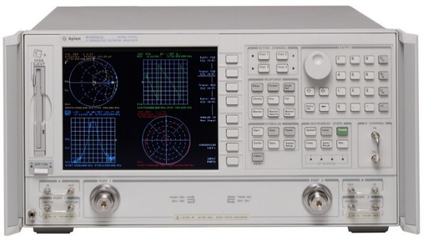
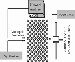
The HP (Agilent) 8722ES vector network analyzer includes an integrated synthesized source, test set and tuned receiver, and allows complete characterization of RF and microwave components. The built-in S-parameter test set provides a full range of magnitude and phase measurements in both the forward and reverse directions. Built-in vector accuracy enhancement techniques include full two-port, adapter-removal, and optional TRL calibration.
Using the 8722ES network analyzer we can perform (Transmission/Reflection) measurements in the frequency range 50MHz-40GHz, either in free space, or using waveguides, at temperatures varying from RT to ~200°C.
 Our group's website: http://gate.iesl.forth.gr/~ppm/index.html
