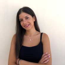
Eirini Katsipoulaki is a PhD student at the Department of Physics at the University of Crete,Greece. She received her Bachelor degree in Physics from University of Crete, Greece in 2019 and her M.sc. in master program "Photonics and Nanoelectronics" from the same department. In 2019, she joined the “Ultrafast Laser Micro and Nano Processing” Group of IESL, FORTH. Her bachelor thesis subject was: “Pulsed laser deposition and characterization of thin films WS2 ”. Her current research interests include two Dimensional Materials (2D), μ-Photoluminescence Spectroscopy (μ-PL), Raman Spectroscopy and Pulsed laser irradiation of the atomically thin lattice in a precursor gas atmosphere. Her research interests, also, lie in the effect of carrier doping.
Education
- 2021 - now : PhD, Department of Physics, University of Crete, Greece
- 2019 - 2021: Master of Science, Physics Department, University of Crete, Greece, 9.38/10
- 2015-2019:Bachelor degree in Physics from University of Crete, Greece, 8.54/10
Career
- September 2020-December 2020: Teaching Assistant as a master student, at the undergraduate course “Advanced Physics Laboratory”, Physics Department, University of Crete. Instructor: Prof. Eleftherios Iliopoulos.
- September 2019-December 2019: Teaching Assistant as a master student, at the undergraduate course “Advanced Physics Laboratory”, Physics Department, University of Crete. Instructor: Dr. Ioannis Karadamoglou
- September 2019-Today: M.Sc. Photonics Nanoelectronics, Department of Physics, University of Crete, Greece - Institute of Electronic Structure & Laser, FORTH
- March 2019-May 2019: Work experience as an undergraduate student at Ultrafast Laser Micro-Nano Processing Laboratory, Institute of Electronic Structure & Laser, FORTH
- March 2019-September 2019: Undergraduate student, Department of Physics, University of Crete, Greece - Ultrafast Laser Micro-Nano Processing Laboratory, Institute of Electronic Structure & Laser, FORTH, Heraklion, Crete, Greece. Bachelor thesis: Pulsed
- September 2018-December 2018: Teaching Assistant as an undergraduate student, at the undergraduate course “Optics Laboratory”, Physics Department, University of Crete. Instructor: Prof. Ioannis Kominis.
- February 2018-May 2018: Teaching Assistant as an undergraduate student, at the undergraduate course “Optics Laboratory”, Physics Department, University of Crete. Instructor: Prof.Theodoros Tzouros .
- February 2017-May 2017: Teaching Assistant as an undergraduate student, at the undergraduate course “Mechanics and Thermodynamics Laboratory”, Physics Department, University of Crete. Instructor: Prof.Andreas Zezas
- September 2016-December 2016: Teaching Assistant as an undergraduate student, at the undergraduate course “Mechanics and thermodynamics Laboratory”, Physics Department, University of Crete. Instructor: Prof.Andreas Zezas
Interests
- Mechanical Exfoliation of Two Dimensional Crystals
- Pulsed laser irradiation in a precursor gas atmosphere
- Raman Spectroscopy
- Micro-Photoluminescence Spectroscopy
- Micro-Differential Reflectance Spectroscopy
- Cryogenic System
Awards/Prizes/Distinctions
- November 2019, Graduation of Physics Department, University of Crete, Second best grade of the Graduation( 8.54/“Arista”)
- First grade of Master program “Photonics and Nanoelectronics” (year of admission 2019-2020)

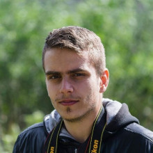
Stamatakis Alexandros is an MSc student at the Inter-institutional Program “Nanotechnology for Energy Applications”. He received his Bachelor in Environmental Engineering from the Polytechnic School of Patras, Greece, in 2019. During his MSc program, he joined the Ultrafast Laser Micro- and Nano- Processing Group of IESL-FORTH for his MSc thesis, working on Advanced Nanomaterials for Water Treatment Applications.
Education
- 2020-Today, MSc student, “Nanotechnology for Energy Applications”, Inter-institutional Postgraduate Program
- 2019- BEng in Environmental Engineering, University of Patras
Career
- 1/9/2020 - Today, MSc Thesis “Advanced Nanomaterials for Water Treatment Applications”, Institute of Electronic Structure & Laser, Foundation for Research and Technology – Hellas
- 1/5/2018 – 1/12/2018, BEng Thesis “Hybrid Reactor Systems for Landfill Leachate Treatment”, Laboratory of Environmental Systems, University of Patras
- 1/7/2018 – 31/8/2018, Bachelor Internship as an Environmental Engineer, Technical Office “Tzoganis Dimitrios”
Interests
- Water Treatment Applications
- Pulsed Laser Deposition
- Laser Ablation in Liquids
- Characterization Techniques (Raman, SEM, TEM, XRD, UV-VIS)
Awards/Prizes/Distinctions
- 1st Graduate of the Department of Environmental Engineering at year 2019.
- Participant of 5th workshop of Chemical Engineering at Patras in 2019 with conference speech “Study of NH4+ removal efficiency on sanitary landfill leachates in lab- and pilot- scale adsorption.
- Distinction in English for achieving over 90% in every section.
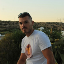
Nikolaos Diakos is a MSc candidate at the “Nanotechnology for Energy Applications” of the Hellenic Mediterranean University (Heraklion, Crete, Greece). He received his in 2017. In 2016, he joined Ultrafast Laser Micro- and Nano- Processing Laboratory of IESL-FORTH, for his Bachelor Thesis entitled “Consecration of periodic structures on Titanium Alley surfaces using an ultra-fast femtosecond laser for biological applicants”. In 2020, he joined the Ultrafast Laser Micro- and Nano- Processing Laboratory of IESL-FORTH group as a master student and his current research interests concern the development of laser based methods for the fabrication of Graphene Related Materials for application in different layers of Perovskite Solar Cells to enhance the efficiency and long term stability of the devices.
Education
- 2019-Today, MSc candidate at the “Nanotechnology for Energy Applications” of the Hellenic Mediterranean University (Heraklion, Crete, Greece).
- 2010-2017, Bachelor of Science (BSc) in Materials Science and Technology, Department of Materials Science and Technology, UoC. (Heraklion, Crete, Greece)
Interests
- Nanotechnology and Nanosciences
- Nanomaterials for energy applications
- Laser – Mater interaction
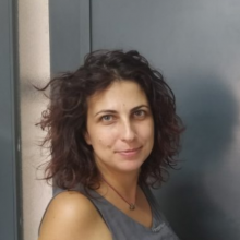
Dr. Dimitra Milioni received her Diploma on Applied Physics from the National Technical University of
Athens (NTUA), Greece and then pursued her studies (M.Sc.) on Molecular and Cellular Biophysics in
Pierre et Marie Curie University – Paris VI, France. She obtained her PhD degree on Biophysics from the
same University (2012). On 2013 she joined the Biosensors group at the Institute of Molecular Biology
and Biotechnology (IMBB-FORTH) until 2020, when she became a member of the Ultrafast Laser Micro-
and Nano- Processing Laboratory.
Her scientific interests lie on biosensors and their use for diagnostic purposes, as well as on the development of new methodologies for biosensor devices. Also, she is interested on model membranes (liposomes, supported lipid bilayers, BLM) and their interaction with other molecules (antimicrobial peptides, membrane proteins & amphiphilic polymers) for drug delivery applications.
Education
- PhD in Life Sciences (November 2012): “Photocontrolled Permeabilization of Biological Membranes; Studies on model membranes and cells”, BioMolecules Lab, Pierre et Marie Curie University, Chemistry dpt (UMR 7203, UPMC-CNRS-ENS), France.
- MSc.: “Molecular and Cellular Biophysics” (June 2009): Physics Faculty, Pierre et Marie Curie University (UPMC-Paris VI), France.
- 5-year Diploma: “Applied Physical Sciences” (July 2008): School of Applied Mathematical and Physical Sciences, National Technical University of Athens (NTUA), Greece.
Career
- Research Associate (September 2020 – today): Ultrafast Laser Micro and Nano Processing Laboratory, Institute of Electronic Structure and Lasers - Foundation for Research and Technology – Hellas (IESL – FORTH), Greece.
- Research Scientist (April 2013 – June 2020): Biosensors Lab, Institute of Molecular Biology and Biotechnology - Foundation for Research and Technology - Hellas (IMBB - FORTH), Greece.
- Postdoctoral Collaborating Researcher (October – December 2016): BioMolecules Lab, “Analysis, Molecular and Cellular Interactions” group, Pierre et Marie Curie University - National Center for Scientific Research - École Normale Supérieure (UMR 7203, UPMC
- Visiting Researcher (December 2012 – March 2013): Molecular Modeling and Drug Design Laboratory (Cournia Lab), Biomedical Research Foundation - Academy of Athens (BRFAA), Athens, Greece.
- Research Engineer (September – November 2012): BioMolecules Lab, “Analysis, Molecular and Cellular Interactions” group, Pierre et Marie Curie University - National Center for Scientific Research - École Normale Supérieure (UMR 7203, UPMC-CNRS-ENS), France
- Teaching Assistant (September 2009 – November 2012): 1st and 2nd semester courses (L1-PCME, LP111), Physics Faculty, Pierre et Marie Curie University (UPMC – Paris VI), France.
Interests
- Biosensors, new methodologies for biosensor devices
- Molecular biophysics
- Nanocarriers, nanoparticles & biological use
- Model membrane systems (liposomes, BLM, SLB)
- Cell membrane permeabilization & intermolecular interactions
- DNA and protein conformational changes & interactions
- Protein adsorption on surfaces, surface chemistry
Awards/Prizes/Distinctions
- 2015 - 2017: Postdoc Fellowship of Excellence by the State Scholarships foundation, Greece (ΙΚΥ-Siemens).
- 2016: French Ministry of National Education, Higher Education and Research. Grant for young researchers («Séjours scientifiques de haut niveau» - SSHN 2016).
- 2013: Qualified for Assistant Professor Positions in Higher Education in France (Section 28: Dense Mediums and Materials).
- 2009: French Ministry of National Education, Higher Education and Research. Research grant for PhD Thesis preparation.
- 2008: Regional Council of Île-de-France. Grant for Master Thesis preparation.
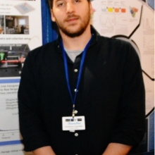
Konstantinos Tsimvrakidis received the Ph.D. in electronics and nanoscale engineering from University of Glasgow, U.K., and an M.Sc. in Nanoscience from University of Strathclyde, U.K. He is currently a Post-Doctoral Researcher with the Ultrafast Laser Micro and Nano Processing Laboratory Group at IESL-FORTH, Crete, Greece, running under the supervision of the director of research Dr. E. Stratakis. His research interests include optics, photonics, optoelectronics, laser spectroscopy, laser material processing.
Education
- 5/2020, Ph.D., “Singlet oxygen luminescence detection” – Department of Electronics and Nanoscale Engineering, University of Glasgow, Glasgow, UK.
- 9/2019, M.Sc. in Nanoscience – Department of Physics & Chemistry, Strathclyde University, Glasgow, UK.
- 7/2014, B.Sc. in Electrical and Electronics Engineering – Technological Educational Institute of Central Greece.
Career
- 12/2020 – Today, Post-doctoral Researcher, Ultrafast Laser Micro and Nano Processing (ULMNP) group, Institute of Electronic Structure and Laser (IESL), Foundation for Research and Technology-Hellas (FORTH), Heraklion, Crete, Greece.
Interests
- Laser material synthesis
- Optics and photonics
- Laser Spectroscopy
- Time-correlated single photon counting techniques
- Single photon detection

Mr. Christos Ntoulias is the Laboratory Manager and Lead Mechanical Engineer at the Ultrafast Laser Micro- and Nano-processing Laboratory (ULMNP) within the Institute of Electronic Structure and Laser (IESL). He holds a Master of Engineering (MEng) from the University of Patras (2019) and has been a key member of the ULMNP team since September 2020. In his current role, Christos leads the design and development of 2D/3D models for custom experimental setups, and oversees the operation and maintenance of the laboratory’s core facilities, including 3D printing, laser systems, and automated equipment.
Education
- 10/2013 -4/2019 Master of Engineering in Mechanical Engineering and Aeronautics department in University of Patras
Career
- 9/2020 – Today Lead Mechanical Design Engineer/Laboratory Manager for Ultrafast Laser Micro-and-Nano-processing Group
- 10/2018-4/2019 – Diploma thesis “SYNTHESIS, CHARACTERIZATION AND MECHANICAL BEHAVIOR OF A 3D-PRINTED BIO-SCAFFOLD” in the Laboratory of Applied Mechanics and Materials Engineering at the University of Patras.
- 7/2017-9/2017 – Internship as Junior Mechanical Engineer in Adamant Composites Ltd
Interests
- CAD/CAM technologies
- Automations for Laser and 3D-printing Experiments
- FEM Analysis
- 3D Printing
- Bioprinting
- Sustainability(LCA)
Education
- 2018, BSc, Department of Chemistry, University of Crete, Greece
- 2020, MSc, Department of Chemistry, University of Crete, Greece
Career
- 2/2021-today, Ph.D. candidate, Department of Chemistry, University of Crete, Greece
Interests
- Self-healing polymers and composites
- Organic-inorganic nanohybrid materials
- Polymer crystallization
- Polymer surfaces and interfaces
- Analytical Chemistry
- Electrochemistry
- Biosensor construction and development


