To: 10/11/2022 14:00
Halide perovskite semiconductors can merge the highly efficient operational principles of conventional inorganic semiconductors with the low‑temperature solution processability of emerging organic and hybrid materials, offering a promising route towards cheaply generating electricity as well as light. Following a surge of interest in this class of materials, research on halide perovskite nanocrystals (NCs) has gathered momentum in the last years. While most of the emphasis has been put on CsPbX3 perovskite NCs, more recently the so-called double perovskite NCs, having chemical formula A+2B+B3+X6, have been identified as possible alternative materials, together with various other metal halides structures and compositions, often doped with different elements. This talk will also discuss the research efforts of our group on these materials. I will highlight how for example halide double perovskite NCs are less surface tolerant than the corresponding Pb-based perovskites. Other topics that will be covered are the role of surface ligands on stabilizing the NCs (including those with alloy compositions), doping, and our ongoing research on various other metal halides (for example the Mn-based ones). I will also show our recent results on the synthesis and advanced characterization of heterostructured nanocrystals in which one domain is a lead chalcohalide and the other domain is a cesium lead halide perovskite.
To: 09/11/2022 14:00
Every few seconds, each of us exhales a rich cocktail of gaseous chemicals into our immediate surroundings. This mixture is quantitatively dominated by nitrogen (74.5 %), oxygen (13.7 %), carbon dioxide (5.3 %) and water vapour (~6 %), but it is the remaining 1 % fraction that earns increasing scientific and medical interest. At these trace levels, exhaled breath is a complex mixture of volatile compounds that derive from internal biochemical processes and can provide potential indications of physiological status, environmental burden, and disease. This lecture will introduce the concept of non-invasive breath analysis as a means for exploring physiological state. After a brief historical overview of detection of disease ‘on the breath’, the talk will introduce state-of-the-art sampling methodologies and analytical technologies, from lab-scale instrumentation to sensor-based devices, and review established breath tests for biomarker detection. The lecture will conclude with a look at current challenges and a prospective outlook of this innovative application in health and disease diagnostics.
Position Description
Μη καταστροφικός χαρακτηρισμός του αριθμού ατόμων υπέρψυχρου νέφους με ακρίβεια στο επίπεδο του θορύβου βολής.
Θα αναπτυχθεί μια διάταξη για τη μέτρηση του αριθμού ατόμων σε ένα υπέρψυχρο ατομικό νέφος χωρίς αύξηση της θερμοκρασίας του. Η μέτρηση βασίζεται στο φαινόμενο Faraday, όπου το φως υπόκειται σε οπτική περιστροφή καθώς διαδίδεται μέσα από ένα σύνολο ατόμων. Θα πραγματοποιηθούν τροποποιήσεις σε μια υπάρχουσα διάταξη που θα μας επιτρέψουν να χαρακτηρίσουμε τον αριθμό ατόμων με ακρίβεια καλύτερη από το επίπεδο θορύβου-βολής. Αυτές περιλαμβάνουν: στροβοσκοπική διαμόρφωση της οπτικής δέσμης που χρησιμοποιείται στην ανίχνευση, και την εισαγωγή μιας οπτικής κοιλότητας για την αύξηση της αλληλεπίδρασης ατόμου-φωτός. Επιπλέον, θα επιδιωχθούν βελτιώσεις στη διαδικασία παραγωγής του υπέρψυχρου νέφους, προκειμένου να επιτευχθεί πιο γρήγορη και αξιόπιστη παραγωγή ατομικών νεφών με μεγαλύτερο αριθμό ατόμων σε σχέση με αυτά που μπορούν να παραχθούν αυτή τη στιγμή στο εργαστήριό μας
Για το πλήρες κείμενο της πρόσκλησης ακολουθήστε τον σύνδεσμο 'Related Documents'
Related Project
QCAT -Required Qualifications
- Μεταπτυχιακό Φυσικής
- Ερευνητική εμπειρία στο αντικείμενο του έργου
Desirable Qualifications
- Πειραματική ερευνητική εμπειρία σε ατομική φυσική
Application Procedure
Στο φάκελο υποβολής της πρότασης θα πρέπει να εμπεριέχονται τα ακόλουθα:
- Αίτηση (Form Greek στην αριστερή στήλη) με αναφορά στον κωδικό της θέσης και στο όνομα του προγράμματος
- Αναλυτικό Βιογραφικό Σημείωμα
- Ευκρινή φωτοαντίγραφα τίτλων σπουδών
- Πρόσφατη βεβαίωση σπουδών υποψήφιου διδάκτορα
ΥΠΟΒΟΛΗ ΠΡΟΤΑΣΕΩΝ
Οι ενδιαφερόμενοι καλούνται να υποβάλουν τις αιτήσεις τους και όλα τα απαραίτητα δικαιολογητικά, ηλεκτρονικά στη διεύθυνση hr@iesl.forth.gr με κοινοποίηση (cc): στον Δρ Γ. Βασιλάκη (gvasilak@iesl.forth.gr). Οι αιτήσεις θα πρέπει να αποσταλούν με την ένδειξη: «Αίτηση στο πλαίσιο του προγράμματος QCAT, της πρόσκλησης εκδήλωσης ενδιαφέροντος με Α.Π. … και κωδικό θέσης … » (όπως αυτός αναφέρεται στον Πίνακα του Παραρτήματος).
Appointment Duration
16 μήνεςFunding
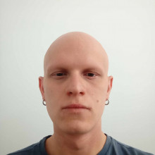
Ioannis Paradeisanos obtained his B.Sc. in 2012 from the University of
Crete in Greece. In September 2014, he completed his Masters’ studies in
micro-optoelectronics at the Physics department of the University of
Crete and in March 2018 he obtained his Ph.D. degree from the same
department. During his Ph.D. dissertation he studied the physics of
different excitonic species in atomically thin semiconductors. After
that, he moved as a postdoctoral research associate to the University of
Cambridge, where he worked on the optical and vibrational properties of
layered materials. From October 2019 to September 2022 he was a member
of the Quantum Optoelectronics group in Toulouse to study the optical
properties of transition metal dichalcogenide monolayers and their
heterostructures. In October 2022 he moved to Crete and IESL/FORTH with
a financial support by the Hellenic Foundation for Research and
Innovation (H.F.R.I.) under the “3rd Call for H.F.R.I. Research Projects
to support Post-Doctoral Researchers.
Education
- 2018, Ph. D. in Exciton Physics, Physics Department, University of Crete, Greece.
- 2014, M. Sc in Micro-Optoelectronics, Physics Department, University of Crete, Greece.
- 2012, B. Sc, Department of Materials Science & Technology, University of Crete, Greece.
Career
- 10/2022 - Today, H.F.R.I. Research Fellow, FORTH-IESL, Greece
- 10/2019 - 09/2022, Senior Research Associate, Quantum Optoelectronics Group, INSA/CNRS, Toulouse, France
- 04/2018 - 09/2019, Research Associate, University of Cambridge, UK
Interests
- Light-matter interactions in 2D semiconductors
- Exciton formation and relaxation
- Spin-valley polarization phenomena
- Exciton-exciton, exciton-phonon, exciton-carrier interactions
- Stark and Zeeman effects
- Interlayer coupling in 2D heterostructures
- Lattice vibrations and phonons
- Near-field interactions
The MOCA collaborative project gathers five research groups in Europe (Germany, France, Italy, Hungary, Greece) funded by their own respective national agencies but selected at the European level in the framework of the QUANTERA program.
The goal of this project is to pave the way for long-distance quantum communications between superconducting quantum (sub)processors with optical photons. We shall develop integrated chips for the conversion between microwave and optical photons using ultracold atomic ensembles. The hybrid chip developed in this project, with atoms simultaneously interacting with microwave and optical cavity fields, could be connected to superconducting quantum processors and fiber optical communication networks for realizing coherent links between distant computational nodes. Our project will demonstrate experimental techniques for microwave to optical conversion that are integrable on chips. The final goal of the project is to evaluate the operation and optimal design of a superconducting atom chip with integrated microwave and optical cavities for the coherent transduction of photons.
Principal Investigator
Funding
Ultracold trapped atoms have recently emerged as one of the most promising physical platforms for digital quantum computing, having already demonstrated systems with more than 200 qubits (the computational unit of a quantum computer) with strong interactions mediated by their highly excited Rydberg states and a clear path to further scalability to thousands of qubits. To develop the next generation of fully programmable and scalable quantum computing systems based on ultracold Rydberg atoms, EuRyQa will bring together four complementary European Rydberg platforms. In this way, the consortium aims to provide a unique European solution for Rydberg-based quantum computing, together with the first pan-European benchmarking and standardisation of the technology.
To achieve the project’s aims, EuRyQa unites partners from academia at the forefront of ultracold-atom-based quantum technology with industrial partners providing complementary expertise on quantum hardware, classical electronics, firmware, and software. EuRyQa is coordinated by the University of Strasbourg (France) and other partners include the SMEs PASQAL (France) and Quantum Machines Technologies (Israel), the University of Stuttgart, the spin-off Qruise GmbH from the Research Centre Jülich, and the consultancy EURICE GmbH (Germany), the University of Amsterdam and the Technical University of Eindhoven (the Netherlands), the research center FORTH (Greece), Associacao Portuguese Quantum Institute (Portugal), and Università degli Studi di Padova (Italy).
EuRyQa project is aimed at establishing Rydberg quantum processors as a leading platform for scalable quantum computing in Europe.
"We will provide a common quantum computing stack for Rydberg atoms, a federated cloud service, solutions to concrete computational problems, and key technology for fault-tolerant quantum computing with Rydberg qubits,” says Prof. Guido Pupillo from the University of Strasbourg, who coordinates EuRyQa. "The success of EuRyQa will be a game changer for Europe in a global competition for quantum computing."
Principal Investigator
Students

Funding
Position Description
Τεχνικός εργαστηρίου με πειραματική εμπειρία σε οπτικές διατάξεις με συστήματα λέιζερ υψηλής ισχύος (excimer & femtosecond) για την κατεργασία οπτικών ινών με σκοπό την ανάπτυξη αισθητήρων. Συγκεκριμένα, πρότερη γνώση σε συστήματα excimer λέιζερ για την εγγραφή φραγμάτων Bragg σε οπτικές ίνες είναι απαραίτητη. Πρότερη γνώση σε θέματα αισθητήρων οπτικών ινών επίσης θεωρείται απαραίτητη.
Για το πλήρες κείμενο της πρόσκλησης ακολουθήστε τον σύνδεσμο 'Related Documents'
Required Qualifications
- Πτυχίο Φυσικής
- Μεταπτυχιακό Φυσικής ή Φωτονικής
- Εμπειρία σε διατάξεις εγγραφής περιοδικών δομών Bragg σε οπτικές ίνες
- Εμπειρία σε αισθητήρες οπτικών ινών
- Εμπειρία σε διατάξεις λέιζερ υψηλής έντασης
- Επαρκής γνώση αγγλικής
Application Procedure
Στο φάκελο υποβολής της πρότασης θα πρέπει να εμπεριέχονται τα ακόλουθα:
- Αίτηση (Form Greek στην αριστερή στήλη) με αναφορά στον κωδικό της θέσης και στο όνομα του προγράμματος
- Αναλυτικό Βιογραφικό Σημείωμα
- Ευκρινή φωτοαντίγραφα τίτλων σπουδών
ΥΠΟΒΟΛΗ ΠΡΟΤΑΣΕΩΝ
Οι ενδιαφερόμενοι καλούνται να υποβάλουν τις αιτήσεις τους και όλα τα απαραίτητα δικαιολογητικά, ηλεκτρονικά στη διεύθυνση hr@iesl.forth.gr με κοινοποίηση (cc): στον Δρ Στ. Πισσαδάκη (pissas@iesl.forth.gr). Οι αιτήσεις θα πρέπει να αποσταλούν με την ένδειξη: «Αίτηση στο πλαίσιο του προγράμματος ΦΑΕΘΩΝ, της πρόσκλησης εκδήλωσης ενδιαφέροντος με Α.Π. … και κωδικό θέσης … » (όπως αυτός αναφέρεται στον Πίνακα του Παραρτήματος).
Appointment Duration
6 μήνεςPosition Description
ΘΕΣΗ 2β
Ο μεταπτυχιακός φοιτητής θα ασχοληθεί στα πλαίσια της Ενότητας Εργασία 3 με την ενσωμάτωση νανοδομών σε πολυουρεθανικές διασπορές (ΕΕ 3.1) και την μελέτη σχηματισμού υμενίων από αυτές με έμφαση στις ιδιότητες αυτοΐασης (ΕΕ 3.2) όπως και στα πλαίσια της Ενότητας Εργασίας 4 με την αξιολόγηση συνταγών που θα παρασκευαστούν βασισμένες στις παραπάνω διασπορές (ΕΕ4.2). Τέλος θα μελετήσει κάποιες τις επιφανειακές ιδιότητες των προιόντων που θα προκύψουν σε πιλοτική κλίμακα (ΕΕ5.2)
ΘΕΣΗ 2γ
Ο μεταπτυχιακός φοιτητής θα ασχοληθεί στα πλαίσια της Ενότητας Εργασία 4 με την αξιολόγηση και την μελέτη των ιδιοτήτων συνταγών που θα παρασκευαστούν βασισμένες σε πολυουρεθανικές διασπορές που περιλαμβάνουν παράγοντες αυτοίασης (ΕΕ4.2) όπως και στα πλαίσια της Ενότητας Εργασίας 5 με την μελέτη των ιδιοτήτων των ρητινών και των παραγόντων αυτοίασης που θα παρασκευαστούν σε πιλοτική κλίμακα (ΕΕ5.1) όπως και τις ιδιότητες των αντίστοιχων τελικών προιόντων (ΕΕ5.2)
Για το πλήρες κείμενο της πρόσκλησης ακολουθήστε τον σύνδεσμο 'Related Documents'
Required Qualifications
ΘΕΣΗ 2β
- Πτυχίο φυσικών επιστημών (φυσική, χημεία, επιστήμη υλικών) ή μηχανικού
- Προηγούμενη εμπειρία σε εργαστήρια μελέτης και χαρακτηρισμού υλικών και ιδιαίτερα πολυμερικών υλικών
- Προηγούμενη εμπειρία στην μελέτη επιφανειακών ιδιοτήτων
- Άριστη γνώση της αγγλικής γλώσσας
ΘΕΣΗ 2γ
- Πτυχίο φυσικών επιστημών (φυσική, χημεία, επιστήμη υλικών) ή μηχανικού
- Προηγούμενη εμπειρία σε εργαστήρια μελέτης και χαρακτηρισμού πολυμερών και γνώση αντίστοιχων τεχνικών
- Προηγούμενη εμπειρία στην μελέτη σύνθετων υλικών
- Άριστη γνώση της αγγλικής γλώσσας
Application Procedure
Στο φάκελο υποβολής της πρότασης θα πρέπει να εμπεριέχονται τα ακόλουθα:
- Αίτηση (Form Greek στην αριστερή στήλη) με αναφορά στον κωδικό της θέσης και στο όνομα του προγράμματος
- Αναλυτικό Βιογραφικό Σημείωμα
- Ευκρινή φωτοαντίγραφα τίτλων σπουδών
- Πρόσφατη βεβαίωση σπουδών μεταπτυχιακού φοιτητή
ΥΠΟΒΟΛΗ ΠΡΟΤΑΣΕΩΝ
Οι ενδιαφερόμενοι καλούνται να υποβάλουν τις αιτήσεις τους και όλα τα απαραίτητα δικαιολογητικά, ηλεκτρονικά στη διεύθυνση hr@iesl.forth.gr με κοινοποίηση (cc): στην Δρ Κ. Χρυσοπούλου (kiki@iesl.forth.gr). Οι αιτήσεις θα πρέπει να αποσταλούν με την ένδειξη: «Αίτηση στο πλαίσιο του προγράμματος SELFNANOPUD, της πρόσκλησης εκδήλωσης ενδιαφέροντος με Α.Π. … και κωδικό θέσης … » (όπως αυτός αναφέρεται στον Πίνακα του Παραρτήματος).
Appointment Duration
7,5 μήνεςPosition Description
Time resolved spectroscopy of nanocomposite materials
For the full announcement, follow the link "Related Documents"
Required Qualifications
- PhD degree in Physical Sciences or Engineering
- At least five years of experience related to the position’s topic
- Scientific publications, relevant to the topic, in international scientific journals
- Experience in projects operation and management
- Fluency in English
Application Procedure
Interested candidates who meet the aforementioned requirements are kindly asked to submit their applications with cc to the Scientific Responsible, Dr Emmanuel Stratakis (stratak@iesl.forth.gr).
In order to be considered, the application must include:
- Application Form (Form Greek or Form English to the left)
- Detailed curriculum vitae (CV) of the candidate
- Scanned Copies of academic titles
Appointment Duration
6 monthsPosition Description
The PhD candidate will work in the framework of WorkPackage 2 on the preparation and the physicochemical characterization of graphitic and other 2D nanomaterials that will be used in aqueous polymer formulations and in the framework of WorkPackage 4 with the development and characterization of the formulations.
For the full announcement, follow the link "Related Documents"
Required Qualifications
- Undergraduate degree in Sciences or Engineering (physics, chemistry, materials science, chemical engineering)
- MSc degree in Sciences
- Experience in the development of graphitic materials and utilization of relevant techniques for their study
- Previous working experience in polymer characterization. Knowledge of relevant methods and techniques
- Excellent knowledge of English language
Application Procedure
Interested candidates who meet the aforementioned requirements are kindly asked to submit their applications to the address (hr@iesl.forth.gr), with cc to Dr Kiriaki Chrissopoulou (kiki@iesl.forth.gr).
In order to be considered, the application must include:
- Application Form (Form Greek or Form English to the left)
- Detailed curriculum vitae (CV) of the candidate
- Scanned Copies of academic titles
- Certificate for enrollment in a PhD program
