The dawn of layered materials with the invention of graphene back in 2004 lead to an entire family of novel materials with favorable properties for electronics, sensing and other applications. The Microelectronics Research Group has initiated research in graphene transistors since 2008 and since then has expanded research in other 2 dimensional and carbon based materials such as graphene, transition metal dichalcogenides as well as carbon nanotubes for electronic applications. The focus has been on four main axons covering material aspects, components for electronics, sensing and the target is integrated systems combining the power of 2D based electronics for applications.
Latest job openings in the group:
- Master student position in METATHERM [1]
- Research assistant position in METATHERM [2]
- Research assistant in METATHERM [3]
- Research Assistant in project METATHERM [4]
- Reserarch Assistant in project SMARTWAVE [5]
Research Topics
The activity concentrates on the sources of high quality material and its manipulation. Two large categories of materials are the focus here:
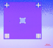
Regarding carbon nanotubes (CNTs) it is critical to control the chirality, diameter, placement and surface functionalization of the nanotubes used in various applications. Our aim so far has been to control surface functionalization and deposition methods in order to create well controlled CNT depositions on various substrates. Those “carpets” as they are called have been used to develop CNT based components such as transistors (CNTFETs) and other. The original material is until now aquired through external collaborations (Chalmers Univ., SHT) or commercial vendors.
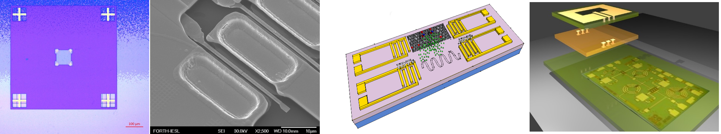
Regarding layered materials (two dimensional materials) the majority of research was originally conducted using exfoliation. The technique was mastered in collaboration with a spin off company of the A.Geim / K.Novoselof group (Graphene industries Ltd). Since 2012 graphene grown on SiC by sublimation (Linkoping University) and CVD grown material (Commercial Graphenea Ltd) was used. Since January 2017 a dual CVD system able to grow graphene and Transition Metal DiChalcogenides (TMDCs) using solid precursors was commissioned. This provided large area material for electronics and other applications. Transfer of 2D materials from the growth substrate to any arbitrary surface has been developed based on a wet process. Finally, chemical liquid exfoliation is still used to provide large volume of nanoflake quality materials used in the 2D based senors
The concept of material with inherently low dimensionality as the core of nano-electronics has been around since the 80’s. Carbon nanotubes have been investigated since their structure is natively inert and they have a quantum wire structure that offer ballistic transport over large distances. With the invention of 2D materials this area has gained enormous attention. Now not only CNTs but also a large pool of monolayer nanomaterials are available for use and above all offer 1D as well as 2D structures with no dangling bonds. Graphene was the first one to exhibit experimentally mobilities in the tenths of thousands but other materials are also promising. The target of this activity is to establish the know how at the component level and harvest the unique properties of each nanomaterial to achieve a series of new electronic components such as transistors, diodes, antennae and other that operate at higher frequencies, consume less power and are more robust and / or smaller than their conventional counterparts. The microelectonrics group has initiated research in this field back in 2008 (first published record 2009) and has since then systematically studied 2D materials and CNTs at the component level. With the aid of several european projects (FP7 and H2020) this activity is currently at the forefront of research with several SotA components.

Two dimensional materials are a promising candidate for sensing applications for several reasons.
Regarding chemical sensors, the form factor of such materials offers a large interaction with the environment. Furthermore specifically graphene offer the particularly rich and well established chemistry of Carbon materials that provide a clear pathway to chemical selectivity. In this area we are the first (in collaboration with European partners) to develop a surface acoustic wave based sensor that can detect acetone, relative humidity and other chemicals that are of importance for food industry and other applications.
Regarding radiation sensors, the fact that graphene has zero bandgap could be considered a disadvantage for several applications (such as graphene FETs) but in this case it offers a unique characteristic: Graphene will absorb any radiation (ranging from THz to the visible). This characteristic has been used to develop to unique sensors, a ballistic transport sensor for GHz (published 2012) and a polariton based THz bolometer recently developed (published 2018). Finally work has begun on photodetecting devices based on TMDC material (both nanoflakes as well as CVD material. This activity is in early stages but complements the remaining spectral range of radiation sensor development.
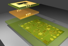
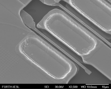
Building on the previous activities, the target is to agglomerate all components into a functional smart nano-system for GHz wireless applications. Circuit level design and integration is the main objective of this activity. Specifically, combining components coming from nanomaterials such as CNT and 2D on the same integrated system (monolithic integration) can provide the best of each technology. This approach also is particularly adapted to the logic of sequential integration, that is combining different materials / tecnhologies on a monolithic approach. In collaboration with THALES, France and a large consortium of partners, we have pursued this logic to create the first nano sized smart wireless transmission and reception integrated circuits based on CNT and Graphene. As the key technology partner in this effort, we have already developed a library of components and a process flow that enables all basic devices (transistors, inductors, capacitors, transmission lines) to be fabricated at the low GHz range based on graphene and CNT technology.
Heads
 [23]
[23]
Technical Staff
 [24]
[24]
 [25]
[25]
 [26]
[26]
 [27]
[27]
Alumni
 [28]
[28]
 [29]
[29]
 [30]
[30]
 [31]
[31]
 [32]
[32]
 [33]
[33]
 [34]
[34]
Infrastructure Equipment

The lab was recently (2015) launched to cover the needs of the activity. The clean room ensures stable Temperature / Humididty environment and is separated in three zones:
Zone 1: General processing
The main target if this zone is to enable hands on access to students (starting from undergraduate) to perform hand on work using basic equipment. This zone is equped with a solvent wet bench, spin coating and hotplates, optical microscopy and profilometry.
Zone 2: RF Characterization
This zone hosts a series of Temperature / humidity sensitive equipment such as RF characterization, a custom Electrical Impedance spectroscopy setup and other characterization tools shown below)
Zone 3: Nanoparticles & 2D growth and manipulation
The last zone focuses on nanoparticle handling (2 nanoparticle tolerant wet benches/hoods with exhaust filtration), a custom made Langmuir Blodgett system, a series of sonicators, precision scales, inert atmosphere glove box, and ovens
In this zone the 2D dual CVD growth system is also placed (Graphenes and Transition metal dichalcogenides)
For information or to request access to the lab please contact George Deligeorgis [35]
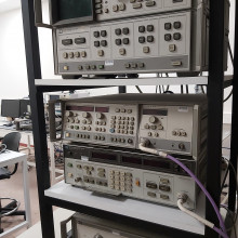
The system aims at characterization of on-wafer or other prototype RF systems.
It is based on the following units:
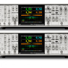
- HP8510c VNA
- custom made high voltage Bias-T (up to 200Volts)
- Keithley 2614B ( High voltage version )
- On-wafer probe station (2 RF probes, aditional DC probes available)
- Labview control using PC
For further information or to request access please contact George Deligeorgis [35]

The system aims at characterization of active components on-wafer or other prototype RF systems.
It is based on the following units:
- Anritsu MS4644B VNA
- Power control option (Performs Compression point analysis)
- Noise figure (Performs Noise figure measurmeent with proper aditional amplifiers)
- Keithley 2604B ( 2 port biasing and current measurement )
- On-wafer probe station (2 RF probes, aditional DC probes available)
- Labview control using PC
For further information or to request access please contact George Deligeorgis [35]
The system was developed in house and is built around a dual lockin setup.
It is capable of measuring:
- Frequency range: 1mHZ - 4 MHz
- Stimuli Voltage range: nVolts - Volts
- Response voltage range: nVolts - Volts
- Current response range: pA - mA
The system can also operate in conjuction with the RF_VNA to cover a range of 9 orders of magnitude in frequency
Measurement can be:
- On wafer (probe station)
- Liquid cell (custom built)
- Temperature cell (under development)
All experiment and data are controlled via dedicated LabView through PC
For further information or to request access / measurements please contact George Deligeorgis [35]

This is a dual chamber Graphene / Transtition metal dichalcogenide CVD system developed by PlanarTECH the system is a planarGROW-2S
The graphene chamber has:
- Quartz 2" growth tube
- SIngle growth zone up to 1100 C
- Heated precursor chamber
- Input gasses are:
- Hydrogen / Methance / Argon
- Automatic
- pressure
- flow
- pump control
- Full recipee mode
The TMD chamber has:
- Quartz 2" growth tube
- Double growth zone each up to 1100 C
- Input gasses are:
- Hydrogen / Argon
- Automatic
- pressure
- flow
- pump control
- Full recipee mode
For more information or to request access / samples please contact George Deligeorgis [35]
We are proud to work with the Libre Space foundation [36] in multiple space related projects:
- We provided consulting in the SatNOGS COMMS [37] project designing a communication platform for CubeSATs and nanosatellites.
- We are also excited to be part of the SidLOC [38] ESA project providing RF design services.